105.11.03 Predictions 2016: contact technology will change connectors

Electroforming contacts is better than stamping and pressing when manufacturing
miniature connectors, writes Hafeez Najumudeen
Whilst semiconductor manufacturers have been halving the size of transistors
roughly every two years, connector manufacturers have been a long way from
keeping pace. One of the reasons is there has been no fundamental change in
contact manufacturing techniques.
Electroforming is a new technique which we at Omron believe overcomes many of
the limitations of stamping and pressing. Not only can smaller, higher quality
and higher performance contacts be manufactured, but the tooling process is much
simpler and cheaper, reducing investment risk and speeding time to market.
What is electroforming?
Electroforming enables high‐precision production of extremely small, thin and
fine patterned contacts. Microfabrication technology allows for considerable
component design flexibility and is also used to meet more exacting needs for
shapes and sizes, since it enables the transfer of a pattern with
submicron‐scale (0.0001 mm) surface roughness accuracy.
Unlike electroplating, electroforming builds thicker, stronger metal layers
which become the actual contact structure.
Electroforming is a metal forming process that forms ultra-thin metal components
through the electroplating process. The components are produced by developing a
layer of metal onto a base form (master). Once the plated layer has been built
up to the desired thickness, the newly formed part is stripped off the master
substrate. Electroforming enables high-precision production of extremely small,
thin and fine patterned parts.
Benefits of EFC
Omron has introduced electroforming technology into the fabrication of the metal
parts of connectors, which were previously formed with presswork. This enabled
forming narrow parts with a high aspect ratio (ratio of thickness and width).
Plates with a width one-third of their thickness have been produced. With
traditional pressed contacts it is difficult to allow the plate width to be less
than the plate thickness.
With electroforming, it is also possible to bend contacts much further.
Traditionally, a plate can be bent to a radius of up to twice the plate
thickness by dynamic mechanical tooling.
Electroforming has achieved a 0.04 mm bend radius by transferring pattern with
static chemical processing. This allows for much more freedom in creating round
shapes, opening new possibilities in component design. This has also allowed
micro slits of 35 microns and holes of 50 microns to be created. These were not
possible with traditional presswork.
With electroformed contact (EFC) technology, burs on cut edges and warping
(undercutting) that are unavoidable with presswork do not occur. A roughness
average (Ra) of as little as 0.1 microns can be achieved with EFC, compared to
typically 3-10 microns with pressed contacts.
In order to reduce the damage to components when attempting to miniaturise them
through press work, soft materials with minimal spring strength have to be used.
However, electroforming can fabricate complex shapes without risk of processing
damage. Therefore, by maximising hardness we can create high spring strength.
Applications of EFC
EFC has already been used to create FPC connectors, battery connectors for smart
phones, slit disks for encoders and miniature probes for semiconductor wafers.
In each case, contacts manufactured with EFC bring greater reliability, improved
performance and further miniaturisation than was possible with press techniques.
For example, in an FPC connector, contact resistance was reduced by 30% from 44
milliohms to 34 milliohms.
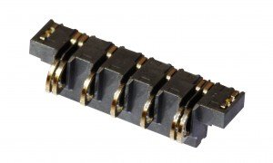
Figure 1: smartphone connector
In smartphone battery connectors (Figure 1), electroformed contacts with
microfabrication achieve a 2 mm pitch and 2.6 mm depth. This compares to a
typical pitch of 2.5 mm and 4 to 5.4 mm depth for pogo pin or pressure style
contacts. While smaller in size, the electroformed contacts are actually less
prone to mechanical fatigue and more shock resistant. Resistance to momentary
power interruptions due to drop impact and repeated vibrations was improved by
30%.
Omron has used electroforming technology in the XD2B line of battery connectors.
This compares to a typical pitch of 2.5 mm and 4 to 5.4 mm depth for pogo pin or
pressure style contacts.
Semiconductor probes
An early area where EFC contacts are already establishing a lead is probe pins
for semiconductors. In recent years, packaging density has been increasing for
surface mount ICs, LCDs, fine-pitch glass substrates, and other electronic
components. This has allowed such components to incorporate more and more
sophisticated functions in electronic equipment.
At the same time, these electronic components have a very large number of pins
and electrode pads, and they are laid out very close to each other on a PCB.
Inspection of electronic components uses a probe pin. Such high-density devices
require inspection of many areas, so multiple probe pins must be placed with a
very small spacing between each. The package unit pitch for recent devices is
only 0.4 to 0.5 mm. In a few years, it is expected to be 0.3 mm or less.
A probe pin is a slender pin-like part that is used to read electric signals
from minute test points when measuring the electrical characteristics of ICs and
other electronic parts. It is a key part that is essential in the test sockets
that hold the ICs in the inspection devices and the probe cards that are built
into the inspection devices.
Using EFC an entirely new style of pin has been created, combining four
components (upper and lower plungers, spring and conductive path) into one. They
have a flat structure which enables placement of pins at any angle, thus making
it easier to reduce pitch compared to a conventional cylindrical probe pin.
The versatility of electroforming technology enables a single component to
incorporate a spring section to provide contact force and durability, and a
barrel section that turns on power when it fits the plunger, separate from each
other. No electricity flows through the miniaturised spring section, thus
solving such problems as excessive temperature rise, the spring section’s
disconnection, and unstable resistance.
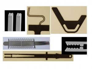
Electroformed contacts come in all shapes and sizes
Since there is no need for costly investment in press dies and other equipment,
as well as the time-consuming die-making process for prototyping and mass
production of probe pins, specific demands for customised non-standard
specifications can be satisfied speedily.
Omron has produced flat probes of 60 microns thickness, and sockets of 150
micron pitch can be assembled. EFC probes can also be very robust. The larger
0.6 mm diameter outer spring type can handle up to 2A. To assemble these tiny
contacts, a special air tweezer tool has been created.
Semiconductor probes are a specialist area of the connector market, but the way
in which EFC has overcome the limitations of press technology is illustrative.
EFC has the potential to transform the connector market (figure 2), enabling the
faster manufacture of prototypes, making smaller production runs economic, and
improving the performance of connectors as well as reducing size. Most of all,
it can create new shapes and styles of connector that we have hardly begun to
imagine.
Hafeez Najumudeen is product marketing manager, Omron Electronic Components
Europe
Article Source:http://www.electronicsweekly.com/news/predictions-2016-contact-technology-will-change-connectors-2016-01/